

GENERAL
Project context and theme
The CdTe detector R&D activity is inherited from the development of the CdTe based imager on board the Integral/Isgri space camera. This R&D programme was classified as a priority R&D study by the Astrophysics department council in November 2002. The activity formally started in February 2003 where SEDI and SAp joined together for this project.
The activity aims at developing segmented electrode arrays based on CdTe or CdZnTe semiconductors ranging from 0.5 up to 6 mm thickness. Both CdTe and CZT are known as possible excellent X and gamma-ray spectrometers, when operated at room temperature or moderately cooled (-40°C up to +30°C).
Until now, performances of such detector types were essentially limited by:
• The crystallographic quality that limits the crystal size, production yield and properties uniformity;
• The poor charge carrier transport properties, subject to charge trapping and ballistic deficit.
Our scientific goal is to progress on all parameters simultaneously. The project is focused on joint progress on spectroscopic performance, spatial resolution and detection efficiency in the high energy range up to 1 MeV to respond to the general expectations of the high energy space science.
On the application side, the project si directly connected with planned high energy astrophysic space missions like the ECLAIRs gamma ray burst detector or the ambitious SIMBOL-X flight-in-formation mission. Recent results of the R&D program led CEA to propose ambitious and credible technical contributions to these space projects, which started phase A in 2005 and 2006 respectively.
Localisation
The project is driven by SAp in the « Space Detector Laboratory » jointly with SEDI in the “Front-end Electronics Laboratory »
Collaboration
The project is connected with the CNES French space agency Research and Technology programme and is open to possible exchanges with ISAS (Japan, Pr. Takahashi) and INFN (Italy, Pr. Fraboni).
Investigation means
Our strategy is to produce in a four year program a prototype of new mini-spectro-imaging device resolved in time, realized according the rules in the space domain. Our demonstrator is a complete mini-gamma camera based on pixelated CdTe or CZT semiconductor, directly connected to its integrated front-end electronics (IDeF-X ASIC family). The prototype named CALISTE is realized in three consecutive steps: the first is to identify and select the accurate technologies and evaluate preliminary prototypes. The next step is to realize a rela full-functional device based on 64 pixels of 1 mm² each. The final step is to realize a full functional prototype with smaller pixel size of about 500 µm square aside. All the prototypes must demonstrate the best achievable spectral response in the 4-300 keV range, in response to the ambitions expectations of the high energy astronomers in our Lab.
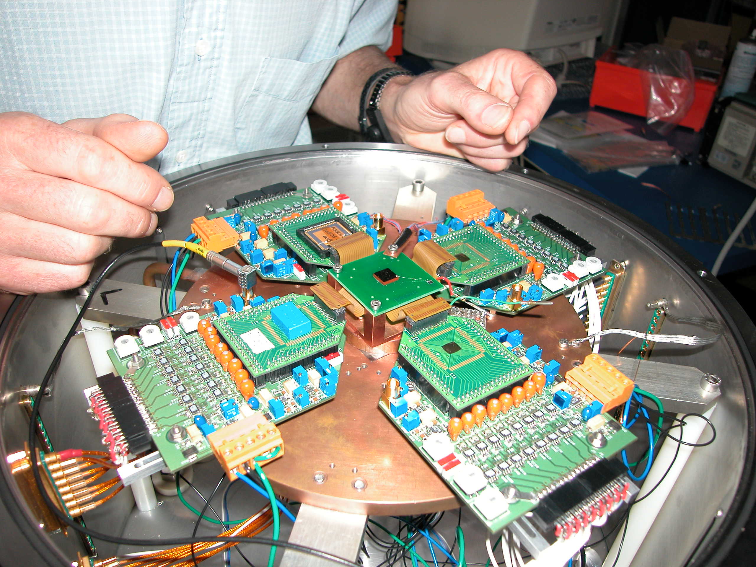
Flat assembly of a CZT Pixelated prototype (1 cm², 2 mm thick), 64 independent pixels of 900 µm square aside readout by IDeF-X V1.0 prototype, a low noise full-custom ASIC
Our Mini gamma camera CALISTE is considered as an hybrid component that may be assembled into a mosaic to form a detector plane of any size and shape. In the frame of the SIMBOL-X mission, the requirement is to cover a 64 cm² area with 16384 pixels, a kind of miniaturized ISGRI.
With 1cm², 0,5-6 mm thick crystals, and an optimised substrate connection with the frontend asics, we expect to reach the following performances:
• 0.6 to 1.2 keV FWHM at 60 keV;
• 400 µm to 750 µm spatial resolution.
Instruments and tools
We use detectors of various types, custom electronics and readout acquisition systems. We also develop 3D modelling tools for detectors from the photon interaction to the signal induction and electronic response.
Specificity
The program is devoted to space instrumentation and all developments are driven by space constraints. The required skillness in asic and electronic development, detector physics simulation, measurement and analysis are all present in the DAPNIA SAp and SEDI Labs.
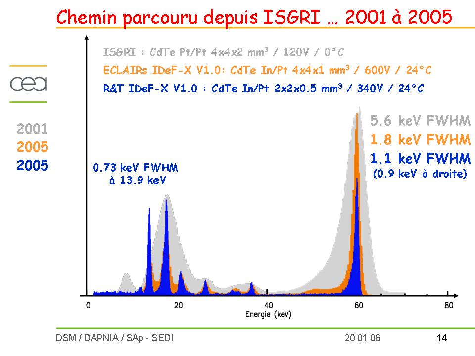
Spectroscopy results obtained in the frame of this R&D as compared with ISGRI, showing a spectacular energy resolution improvement
Status
Important dates
November 2003: first test of new ASIC IDeF-X V0 ;
January 2004: First light of a CdTe detector connected to IDeF-X V0 ;
Summer 2004: Dose tests on IDeF-X V0
Spring 2005: First flat CZT prototype array;
March 2005: New submission of ASIC IDeF-X V1.1
May 2005: Kick off for hybridization activities
Septembre 2005: Measurement campaign on falt CZT prototype connected to IDeF-X V1.0 and crystal at -30°C
October 2005: Record of the laboratory for the spectral response with a Schottky CdTe at +25°C connected to IDeF-X V1.0 (1 keV FWHM at 60 keV, 0.75 keV FWHM at 13.9 keV)
November 2005 : first steps for IDeF-X V1.1
December 2005: First test of IDeF-x V1.0 and CdTe Schottky detectors at -20°C in the frame of ECLAIRs mission.
January 2006: Kick off for the realization of CALISTE 64, first hybrid prototype
February 2006: Dose tests on IDeF-X V1.0 at Cocase; preparation of SEL tests on IDeF-X V1.1
March 2006: Detector mounting on hybrids under control.
June 2006: New ASIC IDeF-X V2 for CALISTE and ECLAIRs.
Status in September 2007:
Chips are very low noise and well suited to our CdTe samples. The CALISTE 64 module started qualification tests in September.
Perspectives
The R&D program goes on and provides SIMBOL-X with technical elements for feasibility studies.
Important facts
We obtained far better spectral response than 1 keV FWHM at 60 keV with new CdTe detectors associated to IDeF-X chip family.
Contact: Olivier LIMOUSIN
• Innovation for detection systems › Detectors for both infinite physics
• The Astrophysics Division (DAp) • The Electronics, Detectors and Computing Division
