The Real-time systems, acquisition electronics and microelectronics laboratory (STREAM) designs and manufactures analogue, digital and programmable electronic components for detection instruments used in experiments conducted by the Institute in various fields.
The laboratory brings together 14 permanent and 6 non-permanent staff in the following fields: analog and mixed analog/digital microelectronics, associated support for characterization, chip bonding and production testing of special-purpose integrated circuits (ASICs), data acquisition system architecture, analog and/or digital electronic board design, firmware programming of field-programmable logic circuits (FPGAs) and embedded real-time system computing.
The STREAM laboratory works in synergy with the Institute’s physics departments and other Sédi laboratories to make significant contributions to leading scientific experiments.
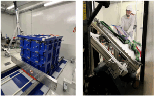
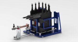
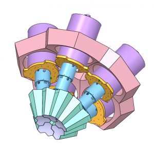
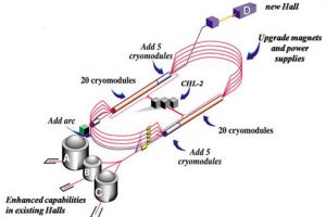
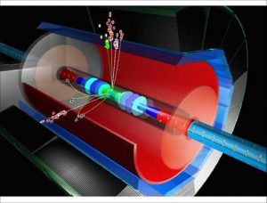
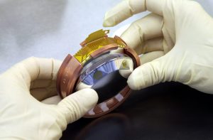
The trajectograph acquisition system for the Clas12 nuclear physics experiment is an example of this combination of skills: the DREAM chip, designed in the STREAM laboratory and based on know-how in low-noise analog microelectronics and analog memories, is the basic building block of the FEU front-end boards, co-developed with Liseta. These cards read cylindrical Micromegas detectors developed at SEDI. This reading system, which will ultimately comprise 20,000 channels, is currently being delivered and installed at Jefferson Lab (USA). On the Franco-Chinese SVOM space mission, STREAM and Lilas laboratories are sharing development of the firmware and on-board software for the satellite’s Scientific and Technical Management Unit (UGTS). The STREAM laboratory also designed and produced the flight ASICs for the ECLAIRs wide-field telescope, a key element of SVOM’s payload. Still for space applications, the STREAM laboratory’s expertise in low-noise radiation-hardened microelectronics enabled it to develop and produce, in collaboration with the astrophysics department, the “Caliste” hybrid micro-gamma camera for the Solar Orbiter satellite.
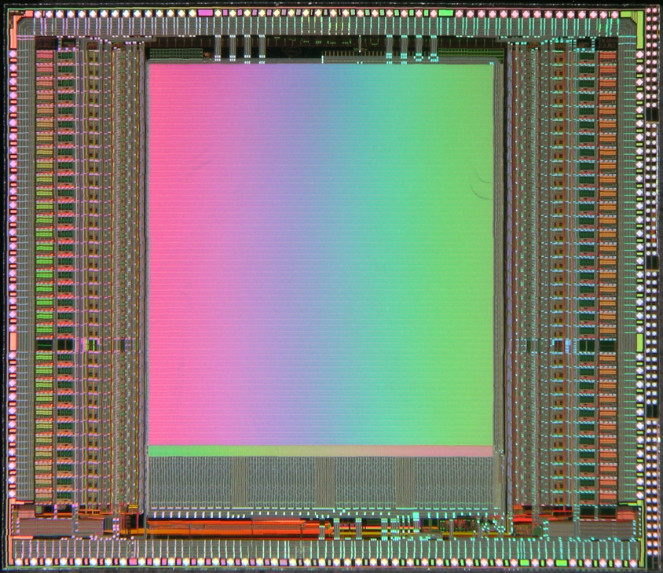
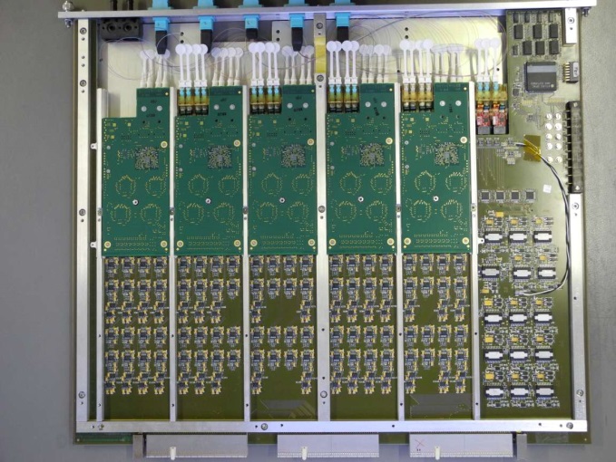
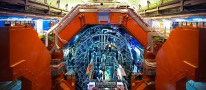
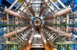
The laboratory’s other main current projects concern Phase 1 of the Large Hadron Collider (LHC) experimental enhancement program at CERN, with a microelectronics contribution to the monolithic pixelated silicon detectors of the ALICE Muon Forward Tracker, and responsibility for the design and production of the 600 or so SOLAR front-end boards for the Bras-Dimuon. In the ATLAS experiment, the STREAM and LISETA laboratories share responsibility with American partners for the design and production of the ~150 high-performance, radiation-hardened “LTDB” digitizing cards.
One of the laboratory’s R&D activities concerns cryogenic microelectronics and the design of superconducting filaments for reading infrared or X-ray bolometer arrays for astrophysics applications.
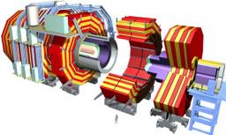
The laboratory is also anticipating the ramp-up to Phase 2 of the LHC experimental enhancement program by developing high-voltage CMOS pixel detectors for the ATLAS internal trajectograph. Similarly, the future front-end ASIC for the central part of the CMS electromagnetic calorimeter is currently being designed in the laboratory.