

Enregistrer dans le calendrier
Quantum bits consisting of single electron or hole spins are realized at CEA-Grenoble on 300mm-wafer industrially compatible CMOS technology.
Their spin state can be manipulated and read-out to build, one-day, a quantum processor. While semiconductor technologies might allow the fabrication of the required thousands of quantum-bits, it also opens valuable possibilities for integrated electronics along with the quantum processor, allowing for better qubit control and higher speed.
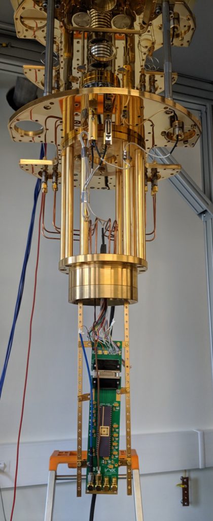
We will present cryogenic circuits designed and tested at CEA-LETI/IRIG using the newly-developed Fully Depleted Silicon-On-Insulator 28nm CMOS technology at temperatures as low as 50mK.
CEA-Leti/IRIG