


R&D maps
MAPS (Monolithic Active Pixel Sensors) are some semiconductor circuits composed of pixels matrix in CMOS technology.
In these matrix, each pixel contains both the detection element and the signal processing circuit.
These componants, in a commercial version, are intend to replace CCDs in few vision equipment (webcam for example).
The main advantage of these componants is the standard technology used for fabrication (cost, disponibility and continuation) and on the possibilities of very fast images processing (up to 1000 per second). On the other hand, performances in sensibility are limited.
This kind of sensors seems to be a good candidate for detectors which need a high granularity and very high precision.
We find these sensors mainly in the vertex detection domain, at the central point of a collider, or in a very fast telescope which need a very good spatial resolution. For these applications, one of the main problem remains the poor detection efficiency. It is limited by the low Silicium thickness of the sensor 'depleted area', by the loose of charge collection and by the fill factor of the chip (insensitive surface occupied with the processing circuit).
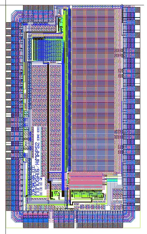
Dapnia department is associated with IPHC institute of Strasbourg (CNRS/IN2P3) to study all these sensor limitations, particularly for the application on the european projet of beam telescope EUDET-JRA1. Dapnia is more precisely in charge to study a conception of fast images transfert circuits and immune to commutation noise. Two prototypes have been already done jointly for the both instituts (2004 and 2006) and the larger prototype delivrable IDC (Intermediate Digital Chip) will be tested in 2008 before the final detector foresee for 2009.
In these matrix, each pixel contains both the detection element and the signal processing circuit.
These componants, in a commercial version, are intend to replace CCDs in few vision equipment (webcam for example).
The main advantage of these componants is the standard technology used for fabrication (cost, disponibility and continuation) and on the possibilities of very fast images processing (up to 1000 per second). On the other hand, performances in sensibility are limited.
This kind of sensors seems to be a good candidate for detectors which need a high granularity and very high precision.
We find these sensors mainly in the vertex detection domain, at the central point of a collider, or in a very fast telescope which need a very good spatial resolution. For these applications, one of the main problem remains the poor detection efficiency. It is limited by the low Silicium thickness of the sensor 'depleted area', by the loose of charge collection and by the fill factor of the chip (insensitive surface occupied with the processing circuit).
Dapnia department is associated with IPHC institute of Strasbourg (CNRS/IN2P3) to study all these sensor limitations, particularly for the application on the european projet of beam telescope EUDET-JRA1. Dapnia is more precisely in charge to study a conception of fast images transfert circuits and immune to commutation noise. Two prototypes have been already done jointly for the both instituts (2004 and 2006) and the larger prototype delivrable IDC (Intermediate Digital Chip) will be tested in 2008 before the final detector foresee for 2009.
#2269 - Last update : 10/25 2007
• Innovation for detection systems › Detectors for both infinite physics
