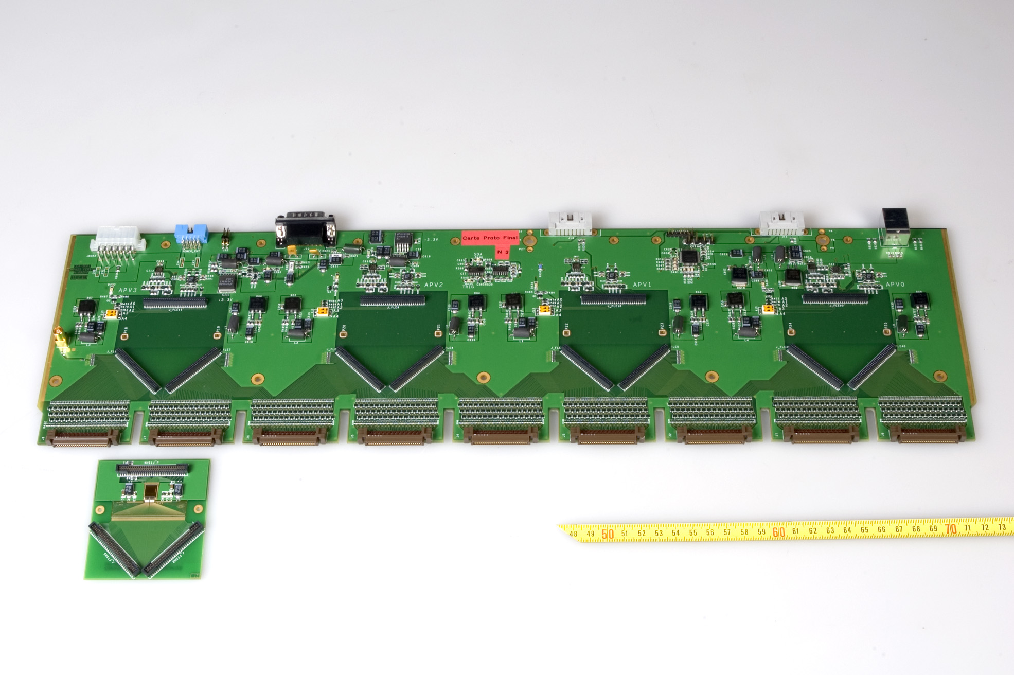
Front-end card used to read RICH detector from the COMPASS experiment. Each motherboard (at top) hosts 4 daughterboards (at bottom) integrating an APV chip processing 128 channels
Although data processing chains are now largely digital, front-end systems - which convert detector signals into electric quantities - remain analogical. For systems requiring a small number of channels, progress made on off-the-shelf circuits leads to ever faster data processing with increased performance. Increasingly fine detector segmentation leads to an increasing number of electronic channels, which itself entails the use of readout microelectronics. In addition to the miniaturization aspect, the use of ASICs (Application-Specific Integrated Circuit) reduces the electric power consumption and the price-per-unit of an electric channel. Although they are essentially comprised of analogical functions, today’s modern ASICs are mixed analogical and digital circuits capable of integrating, for example, sequencers or signal processing functions. Generally-speaking their parameters can be configured. ASICs designed at DAPNIA are classified into three main groups: analogical memories, ultra-low noise circuits, ultra-low consumption circuits and MAPS (Monolithic Active Pixel Sensors).
DAPNIA has over ten years expertise in the field of analogical memories for the high-frequency acquisition of signals with a large dynamic range. SAM, the latest memory designed at DAPNIA, digitizes signals from the HESS-2 experiment at a frequency of one gigahertz and with 12-bit precision. 6,000 copies have been produced so far.
The second group contains IDEF-X circuits developed for CdTe detector-based gamma spectrometry for use in space: the last prototype is designed for the SVOM/ECLAIRs satellite. Acting as a bridge between the first two groups, the AFTER Asic, developed for the T2K neutrino oscillation experiment, includes 72 preamplification and filtering channels and an analogical memory. It is the largest circuit (500,000 transistors) ever to be designed at DAPNIA.
MAPS, part of the third group, connect a detector and its front-end electronics on a single substrate. For the first time, rapid electronics performing highly developed processing tasks have been integrated onto the chips Mimosa 8 and 16 and, as a result, have demonstrated that a MAPS-based trajectograph is feasible for the future colliders. DAPNIA also has considerable expertise in testing and implementing embedded ASICs. New ultra-low noise electronics, based on APV chips designed at the Rutherford Appleton Laboratory, were produced in a very short time-frame to read the 65,000 channels in the RICH detector from the COMPASS experiment.
• Innovation for detection systems › Signal processing and real time systems
• The Electronics, Detectors and Computing Division
• L'expérience COMPASS • SVOM • T2K


